
Blitz Bureau
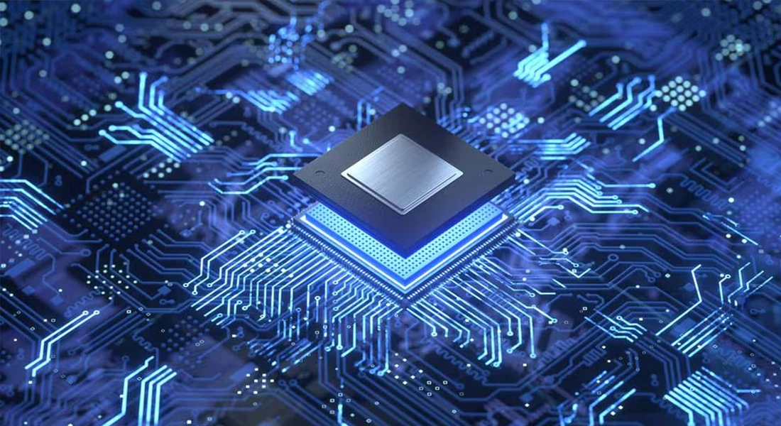
NEW DELHI: The Union Cabinet, chaired by Prime Minister Narendra Modi, on July 15 approved the ‘Semicon 2.0’ scheme for the development of a domestic semiconductor design and manufacturing ecosystem, with a total budget outlay of Rs 1,27,500 crore.
Till date, 12 manufacturing units have been approved with a cumulative investment of over Rs 1.64 lakh crore. These include one silicon fab, one silicon carbide fab, an integrated gallium nitride micro LED display fab and nine packaging units, expected to cater to chip requirements of sectors such as consumer appliances, industrial electronics, automobiles, power electronics, telecommunications, aerospace, etc.
Out of the 12 approved proposals, three companies — Micron, Kaynes and CG Semi — have started commercial production and one more is expected to start in 2026.
Moreover, 24 semiconductor design projects from start-ups and MSMEs have been approved for financial support, while 105 star -ups/MSMEs have been granted access to industry-standard Electronic Design Automation (EDA) tools.
Recognising the requirement to build on the momentum generated under Semicon1.0, Semicon 2.0 aims to further the government’s commitment towards putting our country on the semiconductor map of the world, according to a Cabinet communique.
Semicon 2.0 is aimed at building the semiconductor ecosystem on six pillars.
It will build upon the initial success in chip design. With 105 startups already started developing chips, the focus is on deepening the design ecosystem.
Under Semicon 2.0, the aim is to develop IPs and designs of chips and systems with this approach, the communique said.
The second pillar is ‘Machines and materials.’ Companies involved in the manufacturing and R&D of the machines and manufacturing of materials, chemicals and gases that are essential for manufacturing semiconductors will be incentivised.