
Blitz Bureau
NEW DELHI:India’s semiconductor programme is usually reported as a number of approvals. The more useful number is how many of those approvals have become factories that ship product.
Under the India Semiconductor Mission, approved investment across the sanctioned projects now stands at about ₹1,65,685 crore, spread across six states. Of twelve approved commercial facilities, three are operational and in commercial production — Micron’s assembly, test and packaging plant at Sanand in Gujarat, inaugurated on 28 February 2026, together with CG Semi and Kaynes. That is 25 per cent of the approved set producing, four years into a programme whose first approvals date to 2023. For an industry where a greenfield packaging line takes two to three years and a front-end fab four to five, that is close to schedule rather than behind it.
The distinction that most coverage flattens is the one between the back end and the front end. Micron, CG Semi and Kaynes are ATMP and OSAT operations — assembly, testing, marking and packaging. They take finished wafers made elsewhere and turn them into the chips that go on a circuit board. It is real manufacturing, it employs thousands, and it is where every semiconductor nation starts. It is not, however, chip fabrication. India’s first front-end fab is the Tata–PSMC plant at Dholera, still under construction, designed for 50,000 wafers a month — 600,000 wafers a year — at the 28-nanometre node.
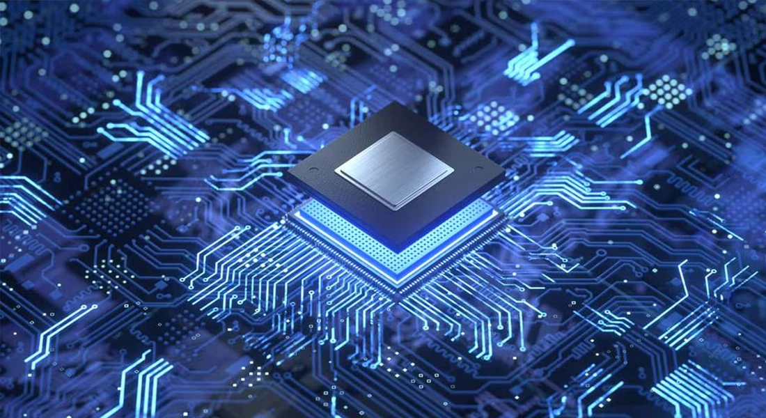
Where the milestone actually sits. A patterned silicon wafer. India’s three operational semiconductor units package chips made elsewhere; the first wafer patterned on Indian soil is expected from the Tata–PSMC fab at Dholera, targeted for December 2026.
Packaging a chip and making one are different industries. India has begun the first and is building the second.
At a Glance
• Approved investment: about ₹1,65,685 crore across six states
• Commercial facilities approved: 12; operational and producing: 3
• Operational: Micron (Sanand, inaugurated 28 February 2026), CG Semi, Kaynes
• First front-end fab: Tata–PSMC, Dholera — under construction
• Dholera capacity: 50,000 wafers a month; 28-nanometre node
• Stated targets: four plants operational by end-2026; two more in 2027
• First silicon from Dholera: targeted December 2026
Twenty-eight nanometres deserves an explanation, because it is routinely misread as a compromise. The most advanced logic in the world is made at three and two nanometres, and India is not attempting that. But the 28nm node is the workhorse of the automotive, industrial, power-management and display-driver markets — the chips in a car’s engine controller, a factory sensor, a washing machine, an inverter. That segment is enormous, it is growing with electrification, and it is where a new entrant can win business on reliability and price rather than on being first to a node. Choosing 28nm is not settling for less; it is choosing the part of the market where a first fab can actually sell what it makes.
The remaining challenge is the layer beneath the fabs, and it is the one to watch over the next two years. A fab consumes ultra-pure chemicals, specialty gases, photoresists, masks and precision equipment, most of which India currently imports — and it needs process engineers in numbers the country has not previously trained. The stated roadmap is four plants operational by the end of 2026, two more in 2027, and first silicon from Dholera in December this year. If those dates hold, the meaningful test arrives in 2027, when the question stops being how many units were approved and becomes how much of each chip’s value is added in India. That figure — domestic value addition per wafer — is the one worth asking for, and worth publishing.